Title: TE0820-04-4AE21FA - Xilinx Tri-Mode Ethernet MAC - RGMII Issue
Post by: toulgaridis on February 10, 2021, 11:14:47 AM
Post by: toulgaridis on February 10, 2021, 11:14:47 AM
Hi,
I am designing an architecture utilizing the AXI 1G/2.5G Ethernet Subsystem (including the evaluation license for the Xilinx TEMAC Core) for the TE0820 FPGA Board.
Block Design is shown in the respective Figure1.
The Hardware configuration is the following:
CarrierBoard: TE0706-03 (https://shop.trenz-electronic.de/en/TE0706-03-TE0706-Carrierboard-for-Trenz-Electronic-Modules-with-4-x-5-cm-Form-Factor)
FPGA Board: TE0820-04-4AE21FA (https://shop.trenz-electronic.de/en/TE0820-04-4AE21FA-MPSoC-Module-with-Xilinx-Zynq-UltraScale-ZU4CG-1E-2-GByte-DDR4-SDRAM-4-x-5-cm)
I am using the J2A RJ45 Ethernet Port (SCH-TE0706-03, page 4 - https://wiki.trenz-electronic.de/display/PD/TE0706+TRM).
According to the TRM and the schematic documentation, this port is connected to the ETH PHY 88E1512 U6 and the RGMI Interface is connected to specific pins of the HP BANK 65 of the TE0820 Zynq Ultrascale Plus FPGA.
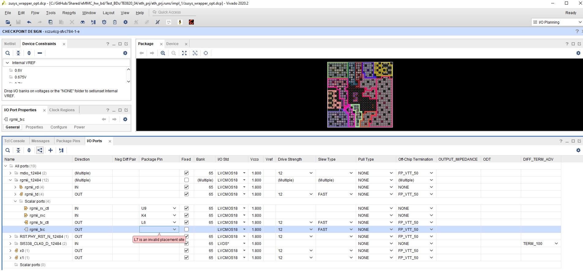
I have an issue assigning the rgmii_txc clock signal (on the FPGA design side) at the L7 PAD (IO_L13P_T2L_N0_GC_QBC_65, B65_L13_P) of the FPGA.
VIVADO gives me the following messages:
1) L7 is an invalid placement site, Figure2.
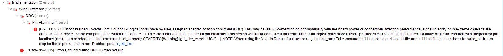
2) The invalid assignment results in the DRC Error, Figure3
Any ideas on how to resolve this issue? Is there any incompatibility matter that I am missing?
I would appreciate your contribution.
Best regards,
Nikolaos Toulgaridis
Researcher
University of Patras
Greece
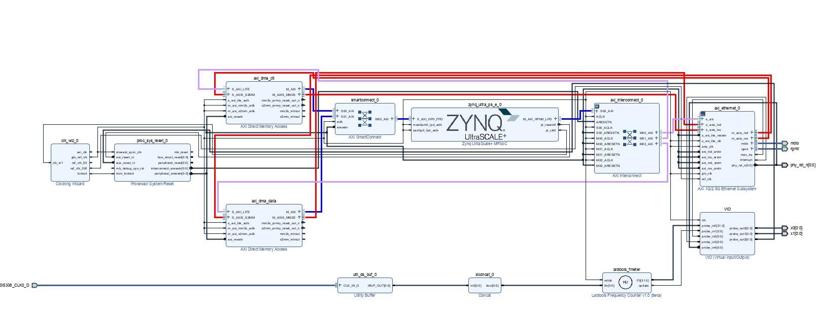
I am designing an architecture utilizing the AXI 1G/2.5G Ethernet Subsystem (including the evaluation license for the Xilinx TEMAC Core) for the TE0820 FPGA Board.
Block Design is shown in the respective Figure1.
The Hardware configuration is the following:
CarrierBoard: TE0706-03 (https://shop.trenz-electronic.de/en/TE0706-03-TE0706-Carrierboard-for-Trenz-Electronic-Modules-with-4-x-5-cm-Form-Factor)
FPGA Board: TE0820-04-4AE21FA (https://shop.trenz-electronic.de/en/TE0820-04-4AE21FA-MPSoC-Module-with-Xilinx-Zynq-UltraScale-ZU4CG-1E-2-GByte-DDR4-SDRAM-4-x-5-cm)
I am using the J2A RJ45 Ethernet Port (SCH-TE0706-03, page 4 - https://wiki.trenz-electronic.de/display/PD/TE0706+TRM).
According to the TRM and the schematic documentation, this port is connected to the ETH PHY 88E1512 U6 and the RGMI Interface is connected to specific pins of the HP BANK 65 of the TE0820 Zynq Ultrascale Plus FPGA.
I have an issue assigning the rgmii_txc clock signal (on the FPGA design side) at the L7 PAD (IO_L13P_T2L_N0_GC_QBC_65, B65_L13_P) of the FPGA.
VIVADO gives me the following messages:
1) L7 is an invalid placement site, Figure2.
2) The invalid assignment results in the DRC Error, Figure3
Any ideas on how to resolve this issue? Is there any incompatibility matter that I am missing?
I would appreciate your contribution.
Best regards,
Nikolaos Toulgaridis
Researcher
University of Patras
Greece
Title: Re: TE0820-04-4AE21FA - Xilinx Tri-Mode Ethernet MAC - RGMII Issue
Post by: JH on February 10, 2021, 11:27:15 AM
Post by: JH on February 10, 2021, 11:27:15 AM
Hi,
we never test this combination with xilinx AXI 1G/2.5G IP (maybe there are some special restriction from Xilinx (Check IP maybe there are some advanced setting to change this)).
We have only TE0720 Reference design with TEB0706, where we use Zynq GEM with MIIto RGMII IP:
https://wiki.trenz-electronic.de/display/PD/TE0720+ETH0706#TE0720ETH0706-BlockDesign
Source code of the Design is available on the download area:
https://wiki.trenz-electronic.de/display/PD/TE0720+ETH0706#TE0720ETH0706-Download
I think the same should work with TE0820 (use correct Pin assigned for TE0820).
br
John